
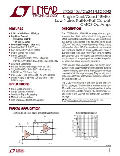
The LTC6240, LTC6241 and LTC6242 are single, dual and quad CMOS operational amplifiers offering ultra‑low noise (0.1 Hz‑10 Hz noise of 550 nVpp), low input bias current (0.2 pA typ, 1 pA max for LTC6240) and rail‑to‑rail output swing within 30 mV of the supply rails. They are designed for high‑performance signal‑processing tasks such as photodiode amplification, charge‑coupled device readout, medical instrumentation and high‑impedance transducer interfaces.
These devices are available in multiple packages (5‑pin SOT‑23, 8‑pin SO, 8‑pin DFN, 16‑pin SSOP, etc.) and operate from 2.8 V to 6 V (standard) or up to 5.5 V for HV versions. Detailed electrical characteristics include a 18 MHz gain‑bandwidth product, 10 V/µs slew rate, and low input capacitance, making them suitable for fast, low‑distortion applications.
| Noise (0.1 Hz‑10 Hz) | 550 nVpp |
|---|---|
| Input Bias Current | 0.2 pA typ, 1 pA max (LTC6240) |
| Input Offset Voltage | 125 µV max |
| Gain Bandwidth Product | 18 MHz |
| Supply Voltage Range (standard) | 2.8 V to 6 V |
The LTC6240/LTC6241/LTC6242 have a noise of 550 nVpp measured from 0.1 Hz to 10 Hz.
The standard LTC6240 operates from 2.8 V to 6 V, while the HV version operates up to 5.5 V.
The LTC6241 is offered in an 8‑pin SO package and a tiny dual‑fine‑pitch leadless (DFN) package.
The LTC6240 has an input bias current of 0.2 pA typical and up to 1 pA maximum.