
The LTC6240/6241/LTC6242 series are low noise, low offset, unity gain stable CMOS op amps featuring 1pA of input bias current. Input bias current is guaranteed to be 1pA max on the single LTC6240. The 0.1Hz to 10Hz noise of only 550nVP-P, along with an offset of just 125µV are significant improvements over traditional CMOS op amps. Additionally, noise is guaranteed to be less than 10nV/√Hz at 1kHz. An 18MHz gain bandwidth, and 10V/µs slew rate, along with the wide supply range and low input capacitance, make them perfect for use as fast signal processing amplifiers. These op amps have an output stage that swings within 30mV of either supply rail to maximize the signal dynamic range in low supply applications. The input common mode range extends to the negative supply. They are fully specified on 3V and 5V, and an HV version guarantees operation on supplies up to ±5V. The LTC6240 is available in the 8-pin SO and the 5-pin SOT-23 packages. The LTC6241 is available in the 8-pin SO, and for compact designs it is packaged in a tiny dual fine pitch leadless (DFN) package. The LTC6242 is available in the 16-Pin SSOP as well as the 5mm × 3mm DFN package.
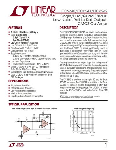
The LTC6240, LTC6241 and LTC6242 are low‑noise, low‑offset, rail‑to‑rail output CMOS op‑amps available in single, dual and quad configurations. They feature 1 pA input bias current (0.2 pA typical) and a gain‑bandwidth product of 18 MHz, making them suitable for high‑speed, low‑noise signal processing.
The document lists absolute maximum ratings, package and order information, detailed electrical characteristics, and typical application circuits such as photodiode amplifiers and low‑noise signal processing stages. Package options include SOT‑23, SO, DFN and SSOP with recommended solder pad layouts.
| Input Bias Current | 0.2 pA typ (1 pA max for LTC6240) |
|---|---|
| Input Offset Voltage | 125 µV max |
| Gain Bandwidth Product | 18 MHz |
| Slew Rate | 10 V/µs |
| Input Noise Voltage (0.1 Hz‑10 Hz) | 550 nV p‑p |
| Operating Temperature Range | ‑40 °C to 125 °C |
The LTC6240 has an input bias current of 0.2 pA typical at 25 °C and a maximum of 1 pA.
All three devices have a gain‑bandwidth product of 18 MHz.