
FDP6035L/FDB6035L N-Channel Logic Level Enhancement Mode Field Effect Transistor is a low voltage application N-channel logic level enhancement mode power field effect transistor produced by Fairchild Semiconductor Corporation. Its features are low on-state resistance, fast switching speed, low inline power loss and resistance to transients.
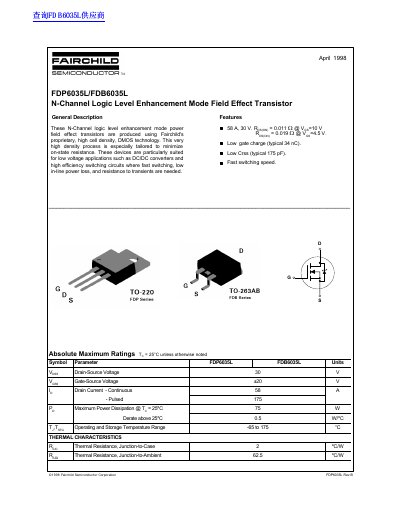
The document describes N-Channel logic level enhancement mode power field effect transistors produced using Fairchild's proprietary, high cell density, DMOS technology. These devices are tailored to minimize on-state resistance and are particularly suited for low voltage applications such as DC/DC converters and high efficiency switching circuits where fast switching is needed.
The datasheet provides absolute maximum ratings, electrical characteristics including drain-source avalanche energy and breakdown voltages, thermal characteristics, typical electrical performance graphs, and safe operating area curves. It covers both the FDP6035L and FDB6035L series available in TO-220 and TO-263AB packages.
| Drain-Source Voltage (Voss) | 30 V |
|---|---|
| Gate-Source Voltage (Vgs) | 420 V |
| Continuous Drain Current (ID) | 58 A |
| Pulsed Drain Current (IDM) | 175 A |
| Maximum Power Dissipation @ Tj=25°C | 75 W |
| Operating and Storage Temperature Range | -65 to 175 °C |
| Thermal Resistance, Junction-to-Case (RthJC) | 2 °C/W |
The typical on-state resistance is 0.011 Ω at Vgs=10V and 0.019 Ω at Vgs=4.5V.
The maximum drain-source avalanche energy for a single pulse with Von=15V and Id=21A is 150 mJ.
The FDP6035L and FDB6035L series are available in TO-220 and TO-263AB packages.