
FDP7030L and FDB7030L are Fairchild's high density DMOS N-Channel logic level enhancement mode power field effect transistors. These devices are particularly suited for low voltage applications such as DC/DC converters and switch mode power supplies.
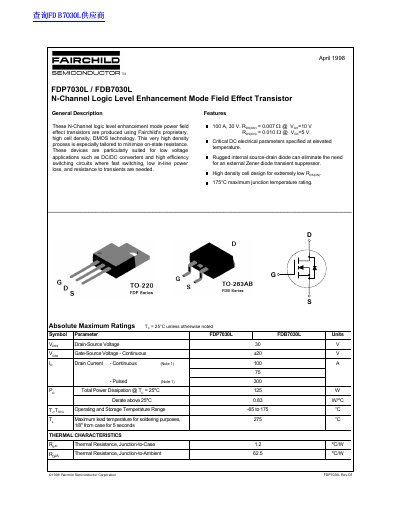
This document is a datasheet for the Fairchild FDP7030 L and FDB7030 L N-Channel Logic Level Enhancement Mode Field Effect Transistors. These devices are produced using Fairchild's proprietary, high cell density, DMOS technology and are particularly suited for low voltage applications such as DC/DC converters and high efficiency switching circuits where fast switching, low in-line power loss, and resistance to transients are needed.
The document provides detailed information about the electrical characteristics, thermal characteristics, absolute maximum ratings, and typical electrical characteristics of the devices. It includes specifications for drain-source voltage, continuous and pulsed drain current, total power dissipation, and operating temperature ranges.
| Drain-Source Voltage | 30 V |
|---|---|
| Gate-Source Voltage | ±20 V |
| Total Power Dissipation | 125 W |
| Operating Temperature Range | -65 to 175 °C |
| Thermal Resistance, Junction-to-Case | 1.2 °C/W |
| Static Drain-Source On-Resistance | 0.007 Ω |
These devices are particularly suited for low voltage applications such as DC/DC converters and high efficiency switching circuits.
The maximum junction temperature rating is 175°C.
No, the rugged internal source-drain diode can eliminate the need for an external Zener diode transient suppressor.