
The PI74SSTU32866 is a 25-bit 1:1 or 14-bit 1:2 configurable registered buffer with parity. It is designed for 1.7 V to 1.9 V VDD operation and supports DDR2-533/400. All clock and data inputs are compatible with the JEDEC standard for SSTL_18. The control and reset (RST) inputs are LVCMOS. All data outputs are 1.8 V CMOS drivers that have been optimized to drive the DDR-II DIMM load, and meet SSTL_18 specifications. The error (QERR) output is 1.8 V open-drain driver.
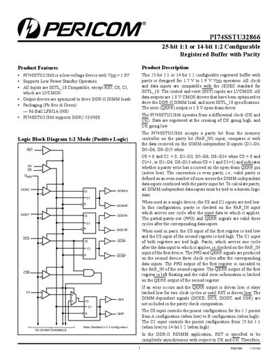
The PI74SSTU32866 is a low‑voltage, 25‑bit 1:1 or 14‑bit 1:2 configurable registered buffer with parity, designed for 1.7 V‑1.9 V Vpp operation. All inputs follow the SSTL_18 standard except the reset and configuration pins, which are LVCMOS. Output drivers are 1.8 V CMOS optimized for DDR‑II DIMM loads, and the device supports low‑power standby mode.
The part is supplied in a 96‑ball LFBGA (NB) package, with detailed pin‑out tables for both 1:1 and 1:2 configurations, functional tables, and parity logic diagrams. Ordering information, mechanical dimensions, and thermal characteristics are also included.
| Power Supply Voltage (Vpp) | 1.8 V nominal |
|---|---|
| Input Compatibility | SSTL_18 (except RST, CO, Cl are LVCMOS) |
| Output Driver Type | 1.8 V CMOS drivers optimized for DDR‑II DIMM loads |
| Configurable Buffer Width | 25‑bit 1:1 or 14‑bit 1:2 |
| Package | 96‑ball LFBGA (NB) |
| Low‑Power Standby | Supported |
The device operates from a nominal Vpp of 1.8 V.
It is supplied in a 96‑ball LFBGA (NB) package.
All inputs are SSTL_18 compatible, except RST, CO, and Cl which are LVCMOS.
It can be configured as a 25‑bit 1:1 or a 14‑bit 1:2 registered buffer with parity.