
MAX V Device Handbook
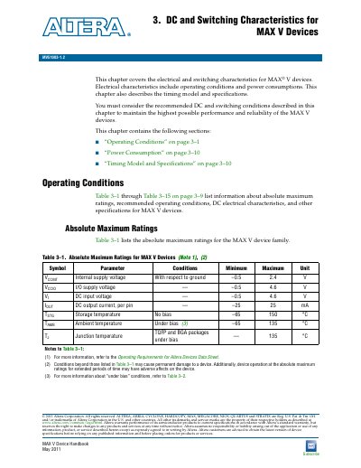
This document provides comprehensive electrical and switching characteristics for the MAX V device family. It covers absolute maximum ratings, recommended operating conditions, power consumption data, and a detailed timing model to ensure optimal performance and reliability.
The text includes specific tables for programming/erasure specifications, DC electrical characteristics such as input leakage currents and supply currents, output drive capabilities across various voltage levels, and I/O standard specifications including 3.3-V LVTTL, LVCMOS, 2.5-V, and 1.8-V standards.
| Internal supply voltage (Vecint) | -0.5 to 2.4 V |
|---|---|
| DC output current per pin | -25 to 25 mA |
| Storage temperature (Tstg) | -65 to 150 °C |
| Ambient temperature (Industrial range) | -40 to 100 °C |
| Configuration flash memory erase cycles | 100 Cycles |
| 3.3-V LVTTL High-level input voltage (Vin) | 1.7 V minimum, 4.0 V maximum |
| 2.5-V I/O supply voltage range | 2.375 to 2.625 V |
The maximum junction temperature (Tj) for BGA packages is 135 °C.
The recommended I/O supply voltage range is 3.00 V to 3.60 V.
The configuration flash memory supports up to 100 erase and reprogram cycles.
Yes, all pins including clock, I/O, and JTAG pins may be driven before Veciyr and Veqig are powered.