
The document describes the absolute maximum ratings and thermal characteristics of the NDS9952A dual N&P-channel enhancement mode field effect transistor released in February 1996. The product is produced using high-density DMOS technology and features low on-state resistance, superior switching performance, and resistance to high-energy pulses. It is particularly suitable for low voltage applications such as notebook computer power management and other battery powered circuits.
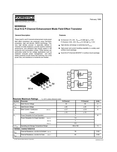
The NDS9952A is a dual N- and P-channel enhancement mode power field effect transistor produced using Fairchild's proprietary, high cell density, DMOS technology. These devices are particularly suited for low voltage applications such as notebook computer power management and other battery powered circuits where fast switching, low in-line power loss, and resistance to transients are needed.
| N-Channel Drain Current (Continuous) | 3.7 A |
|---|---|
| P-Channel Drain Current (Continuous) | -2.9 A |
| N-Channel Drain-Source Voltage | 30 V |
| P-Channel Drain-Source Voltage | -30 V |
| Operating and Storage Temperature Range | -55 to 150 °C |
| Thermal Resistance, Junction-to-Ambient | 78 °C/W |
| Thermal Resistance, Junction-to-Case | 40 °C/W |
The typical on-state resistance for the N-Channel is 0.082 Ω at Vgs=10V.
The typical on-state resistance for the P-Channel is 0.13 Ω at Vgs=-10V.
The maximum power dissipation for dual operation is 2 W.