
This document is a product manual, which introduces the characteristics of QFET products.
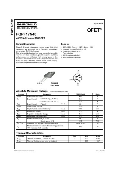
This document provides design specifications and electrical characteristics for the FQPF17N40, an N-Channel MOSFET produced using Fairchild's proprietary planar stripe DMOS technology. The device is optimized to minimize on-state resistance while providing superior switching performance and high energy pulse withstand capability in avalanche and commutation modes.
The datasheet details absolute maximum ratings, electrical characteristics including off and on states, dynamic parameters such as capacitance and gate charge, and typical characteristic curves for voltage, current, and temperature variations. It also includes package dimensions for the TO-220F case.
| Drain-Source Voltage (V_DSS) | 400 V |
|---|---|
| Continuous Drain Current (I_D) at Tj=25°C | 9.5 A |
| Continuous Drain Current (I_D) at Tj=100°C | 6.0 A |
| Pulsed Drain Current (I_DM) | 38 A |
| Gate Threshold Voltage (V_GS(th)) | 3.0 - 5.0 V |
| Static Drain-Source On-Resistance (R_DS(on)) | 0.21 - 0.27 Ω |
| Input Capacitance (C_iss) | 1800 - 2300 pF |
| Total Gate Charge (Q_g) | 45 - 60 nC |
| Power Dissipation (P_D) at Tc=25°C | 56 W |
The maximum drain-source breakdown voltage is 400 V.
The device is packaged in a TO-220F case.
The typical total gate charge is 45 nC.