
The document describes the features and characteristics of a specific model of product, including parameters such as drain-source breakdown voltage, on-state drain current, drain-source on-state resistance, zero gate voltage drain current, etc.
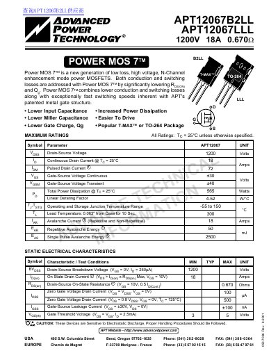
This document describes the Power MOS 7™ family of devices from Advanced Power Technology. These are new generation low loss, high voltage, N-Channel enhancement mode power MOSFETS designed to address both conduction and switching losses by significantly lowering Rds(on) and Qg. The technology combines lower losses with exceptionally fast switching speeds inherent with the manufacturer's patented metal gate structure.
The datasheet provides detailed electrical characteristics for two specific models: APT12067B2LL (T-MAX™ package) and APT12067LLL (TO-264 package). Key specifications include a drain-source breakdown voltage of 1200 Volts, a continuous drain current of 18 Amps, and an on-state resistance of 0.670 Ohms. The document also includes dynamic characteristics such as input/output capacitance, gate charge, and switching times, along with thermal ratings and package outlines.
| Drain-Source Voltage | 1200 Volts |
|---|---|
| Continuous Drain Current | 18 Amps |
| Pulsed Drain Current | 72 Amps |
| Drain-Source On-State Resistance | 0.670 Ohms |
| Total Power Dissipation | 565 Watts |
| Operating Junction Temperature Range | -55 to 150 C |
The maximum continuous drain current is 18 Amps when the temperature is 25°C.
The total power dissipation is rated at 565 Watts when the temperature is 25°C.
The device operates and stores within a junction temperature range of -55 to 150 C.