
This document describes the features and characteristics of FDME1034CZT Complementary PowerTrench® MOSFET, including the maximum on-state resistance of the N-channel and P-channel, low profile design, halogen-free and antimony oxide-free, HBM ESD protection, etc.
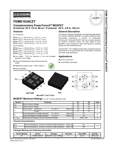
The FDME1034CZT is a complementary PowerTrench MOSFET designed as a single package solution for DC/DC switching applications in ultra-portable devices like cellular handsets. It integrates an N-channel MOSFET and a P-channel MOSFET with low on-state resistance to minimize conduction losses.
The device is housed in a MicroFET 1.6x1.6 Thin package with a low profile of 0.55 mm maximum. It features high HBM ESD protection levels greater than 1600 V and is RoHS compliant. The datasheet provides electrical characteristics, typical performance curves, and dimensional outlines for the component.
| Drain to Source Voltage | 20 V / -20 V |
|---|---|
| Package Type | MicroFET 1.6x1.6 Thin |
| Maximum Profile Height | 0.55 mm |
| HBM ESD Protection | > 1600 V |
| Operating Temperature Range | -55 to +150 °C |
The maximum operating and storage junction temperature range is -55 to +150 °C.
The maximum continuous drain current for the N-Channel MOSFET is 3.8 A.
The maximum power dissipation for single operation at 25°C is 1.4 W.
The maximum operating and storage junction temperature range is -55 to +150 °C.