
The MC10EL/100EL15 is a low skew 1:4 clock distribution chip designed explicitly for low skew clock distribution applications. The device can be driven by either a differential or single-ended ECL or, if positive power supplies are used, PECL input signal. If a single-ended input is to be used the VBB output should be connected to the CLK input and bypassed to ground via a 0.01µF capacitor. The VBB output is designed to act as the switching reference for the input of the EL15 under single-ended input conditions, as a result this pin can only source/sink up to 0.5mA of current. The EL15 features a multiplexed clock input to allow for the distribution of a lower speed scan or test clock along with the high speed system clock. When LOW (or left open and pulled LOW by the input pulldown resistor) the SEL pin will select the differential clock input. The common enable (EN) is synchronous so that the outputs will only be enabled/disabled when they are already in the LOW state. This avoids any chance of generating a runt clock pulse when the device is enabled/disabled as can happen with an asynchronous control. The internal flip flop is clocked on the falling edge of the input clock, therefore all associated specification limits are referenced to the negative edge of the clock input. • 50ps Output-to-Output Skew • Synchronous Enable/Disable • Multiplexed Clock Input • 75kΩ Internal
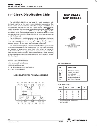
The Motorola MC10EL15 and MC100EL15 are low skew 1:4 clock distribution chips designed for low skew clock distribution applications. The device can be driven by either a differential or single-ended ECL or, if positive power supplies are used, PECL input signal. It features a multiplexed clock input to allow for the distribution of a lower speed scan or test clock along with the high speed system clock.
| Output-to-Output Skew | 50ps |
|---|---|
| Package Type | Plastic SOIC |
Yes, if positive power supplies are used, PECL input signal can be used.
When LOW, the SEL pin selects the differential clock input.
Yes, the common enable is synchronous so outputs are only enabled/disabled when they are already in the LOW state.