
The MC100LVEL/EL91 is a triple PECL to ECL translator. The MC100LVEL91 receives low voltage PECL signals and translates them to differential ECL output signals. The MC100EL91 receives standard voltage PECL signals and translates them to differential ECL output signals. It has features such as low voltage operation, typical propagation delays of 620ps for MC100LVEL91 and 670ps for MC100EL91, fully differential design, and 20-lead SOIC packaging. It also has a VBB output for interfacing with single-ended PECL signals and requires three power rails for level translation. The D input is biased in open input conditions.
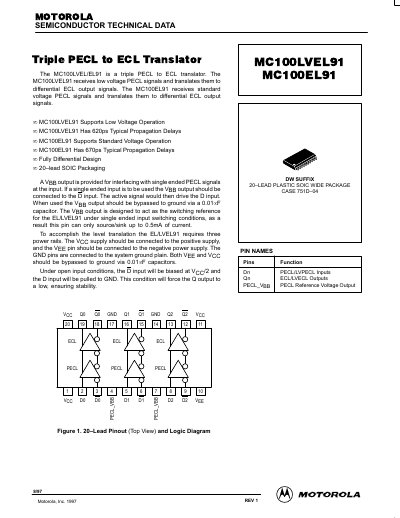
The document describes the MC100LVEL91 and MC100EL91, which are triple PECL to ECL translators. The MC100LVEL91 supports low voltage operation with a typical propagation delay of 620ps, while the MC100EL91 supports standard voltage operation with a typical propagation delay of 670ps. Both devices feature a fully differential design and come in a 20-lead SOIC package.
| Package Type | 20-lead SOIC |
|---|---|
| Typical Propagation Delay (MC100LVEL91) | 620ps |
| Typical Propagation Delay (MC100EL91) | 670ps |
| Power Supply Voltage (LVPECL Input) | 3.0V to 3.6V |
| Power Supply Voltage (PECL Input) | 4.75V to 5.25V |
The Vp output is designed to act as the switching reference for the device under single ended input switching conditions.
The VBp output should be bypassed to ground via a 0.01uF capacitor.
The Vp output can only source or sink up to 0.5mA of current.