
The file is a product datasheet of MC10E195/D from Motorola company. MC10E195/D is a programmable delay chip (PDC) designed primarily for clock de-skewing and timing adjustment. It provides variable delay of a differential ECL input transition. The delay section consists of a chain of gates organized as shown in the logic symbol. The first two delay elements feature gates that have been modified to have delays 1.25 and 1.5 times the basic gate delay of approximately 80 ps. These two elements provide the E195 with a digitally-selectable resolution of approximately 20 ps. The required device delay is selected by the seven address inputs D[0:6], which are latched on chip by a high signal on the latch enable (LEN) control. Because the delay programmability of the E195 is achieved by purely differential ECL gate delays the device will operate at frequencies of >1.0 GHz while maintaining over 600 mV of output swing. The E195 thus offers very fine resolution, at very high frequencies, that is selectable entirely from a digital input allowing for very accurate system clock timing. An eighth latched input, D7, is provided for cascading multiple PDC’s for increased programmable range. The cascade logic allows full control of multiple PDC’s, at the expense of only a single added line to the data bus for each additional PDC, without the need for any external gating.
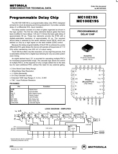
The MC10E195 and MC100E195 are programmable delay chips (PDC) designed primarily for clock de-skewing and timing adjustment. They provide variable delay of a differential ECL input transition using a chain of gates with digitally-selectable resolution.
These devices operate at frequencies greater than 1.0 GHz while maintaining over 600 mV of output swing. The required device delay is selected by seven address inputs (D[0:6]) latched on chip, and an eighth input (D7) allows for cascading multiple chips to increase the programmable range.
| Bandwidth | >1.0 GHz |
|---|---|
| Output Swing | over 600 mV |
| Delay Step Resolution | approximately 20 ps |
| Package Type | PLASTIC PLGG PACKAGE |
It is designed primarily for clock de-skewing and timing adjustment.
The delay is selected by seven address inputs (D[0:6]) which are latched on chip.
Yes, an eighth input (D7) allows for cascading multiple PDCs to increase the programmable range.