
DS90C383/DS90CF384 is a +3.3V programmable LVDS transmitter and receiver for a 24-bit flat panel display (FPD) link. They support a clock frequency of 65 MHz and utilize high-speed data transmission and low voltage differential signaling technology. The transmitter converts 28 bits of LVCMOS/LVTTL data into four LVDS data streams while transmitting a phase-locked clock. The receiver converts the LVDS data streams back into 28 bits of LVCMOS/LVTTL data. They are ideal for solving EMI and cable size problems associated with wide, high-speed TTL interfaces.
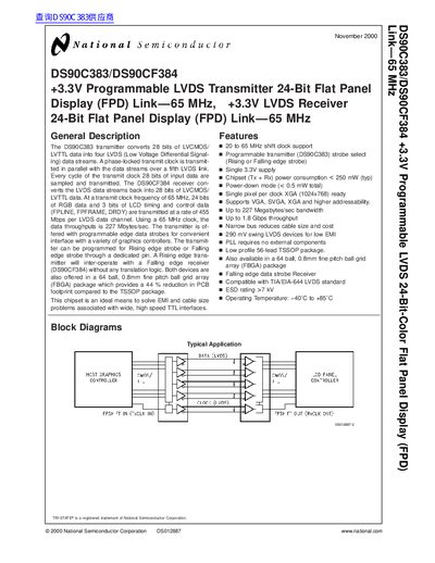
This document describes the DS90C383 transmitter and DS90CF384 receiver chipset designed for +3.3V LVDS applications in Flat Panel Displays (FPD). The DS90C383 converts 28 bits of LYCMOS/LVTTL data into four LVDS data streams, while the DS90CF384 performs the reverse conversion back to 28 bits of data.
The chipset supports a transmit clock frequency up to 65 MHz, enabling a data throughput of up to 1.8 Gbps and a bandwidth of 227 Mbytes/sec for 24-bit RGB data plus timing/control data. It features programmable edge data strobes for the transmitter, compatibility with TIA/EIA-644 LVDS standards, and is available in low-profile TSSOP or FBGA packages.
| Supply Voltage (Vcc) | 3.0 V to 3.6 V |
|---|---|
| Operating Temperature Range | -40°C to +85°C |
| Maximum Package Power Dissipation (TSSOP) | 1.63 W |
| Chipset Power Consumption (Typical) | < 250 mW |
| Power-down Mode Current | < 0.5 mW total |
| Data Throughput | Up to 1.8 Gbps |
| LVDS Output Swing | 290 mV |
The chipset supports a shift clock from 20 MHz to 65 MHz.
Yes, it can be programmed for Rising or Falling edge strobes via a dedicated pin.
The combined Tx and Rx power consumption is typically less than 250 mW.