
This document is a functional block diagram of IDT72T7285, IDT72T7295, IDT72T72105, IDT72T72115. The main features are selectable 2.5V LVTT input and output, support up to 225MHz clock operation, have read enable and read clock echo outputs, and support asynchronous read and write port timing.
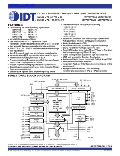
The IDT72T7285, IDT72T7295, IDT72T72105, and IDT72T72115 are exceptionally deep, high-speed CMOS First-In-First-Out (FIFO) memories available in 16,384 x 72, 32,768 x 72, 65,536 x 72, and 131,072 x 72 configurations. These devices support up to 225 MHz operation and feature user-selectable HSTL or LVTTL input and output structures.
| Max Operation Frequency | Up to 225 MHz |
|---|---|
| Memory Depth Configurations | 16,384 x 72 to 131,072 x 72 |
| Package Type | 324-pin Plastic Ball Grid Array (PBGA) |
| Industrial Temperature Range | -40°C to +85°C |
| Input/Output Voltage Options | 2.5V LVTTL or 1.8V, 1.5V HSTL |
The available configurations are 16,384 x 72, 32,768 x 72, 65,536 x 72, and 131,072 x 72.
Yes, the devices feature independent Read and Write Clocks that permit reading and writing simultaneously.
The FIFOs support x72 in to x72 out, x72 in to x36 out, x72 in to x18 out, x36 in to x72 out, and x18 in to x72 out.