
SST 512 Kbit 1 Mbit 2 Mbit 4 Mbit (x8) Multi-Purpose Flash SST39LF512 SST39LF010 SST39LF020 SST39LF040 SST39VF512 SST39VF010 SST39VF020 SST39VF040 Data Sheet

This data sheet introduces the features and characteristics of SST39LF512/010/020/040 and SST39VF512/010/020/040, including organization, voltage range, reliability, power consumption, sector erase capability, read access time, latched address and data, fast erase and byte program, automatic write timing, internal VPP generation, end-of-write detection, CMOS I/O compatibility, and JEDEC standard-Flash EEPROM pin
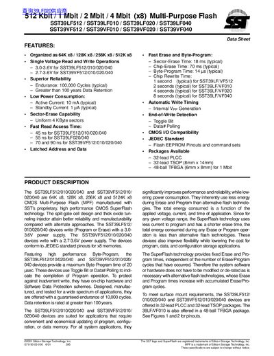

SST 512 Kbit 1 Mbit 2 Mbit 4 Mbit (x8) Multi-Purpose Flash SST39LF512 SST39LF010 SST39LF020 SST39LF040 SST39VF512 SST39VF010 SST39VF020 SST39VF040 Data Sheet - cover page
Brand
SST
Category
Memory
Document type
Datasheet
Language
English
Pages
24
File format
PDF
File size
264 KB
Published
07 June, 2012
Updated
30 September, 2023
MD5 checksum
2913B5CFA9B8341CA2858A3E6C2F1E9F

About this manual

This datasheet describes the SST39LF and SST39VF series of CMOS Multi-Purpose Flash (MPF) manufactured with Silicon Storage Technology's proprietary SuperFlash technology. The devices are organized as 64K, 128K, 256K, or 512K x8 and offer single voltage read and write operations ranging from 3.0-3.6V for LF series to 2.7-3.6V for VF series.

What's inside

  • Features
  • Product Description
  • Device Operation
  • Read
  • Byte-Program Operation
  • Sector-Erase Operation
  • Chip-Erase Operation
  • Write Operation Status Detection

Frequently asked questions

What is the typical endurance of these flash devices?

The devices have a typical endurance of 100,000 cycles.

How long does it take to erase the entire chip?

The typical Chip-Erase time is 70 ms.

What is the maximum Byte-Program time for these devices?

The maximum Byte-Program time is 20 usec.

Download PDF (264 KB)

More SST Manuals


View all SST manuals →