
This document describes the features and characteristics of SST39VF6401B / SST39VF6402B, including organization, single voltage read and write operations, reliability, low power consumption, block protection, sector erase capability, chip erase capability, etc.
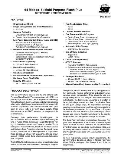
The SST39VF6401B and SST39VF6402B are 64‑Mbit (4M × 16) CMOS Multi‑Purpose Flash Plus devices that operate from 2.7 V to 3.6 V. They feature low power consumption, high endurance (100 k cycles) and long data retention (>100 years). The devices support single‑voltage read/write, auto low‑power mode, and hardware block‑protection.
The datasheet describes command sequences for read, word‑program, sector‑erase, block‑erase and chip‑erase operations, as well as status‑detection methods (Data# polling and toggle bits). It also details hardware and software data‑protection schemes, pin assignments for 48‑lead TSOP and 48‑ball TFBGA packages, and CFI information for system integration.
| Capacity | 64 Mbit (x16) |
|---|---|
| Organization | 4M × 16 |
| Operating Voltage | 2.7 V – 3.6 V |
| Active Current (typical, 5 MHz) | 9 mA |
| Standby Current (typical) | 3 µA |
| Fast Read Access Time | 70 ns – 90 ns |
| Sector‑Erase Time (typical) | 18 ms |
| Block‑Erase Time (typical) | 18 ms |
| Chip‑Erase Time (typical) | 40 ms |
| Word‑Program Time (typical) | 7 µs |
| Package Types | 48‑lead TSOP (12 mm × 20 mm) and 48‑ball TFBGA (8 mm × 10 mm) |
The devices operate from 2.7 V to 3.6 V.
Typical standby current is 3 µA.
They are offered in 48‑lead TSOP and 48‑ball TFBGA packages.