
This document describes the AS7C3364NTF32B and AS7C3364NTF36B products from Alliance Semiconductor. These products are 3.3V 64K×32/36 flowthrough synchronous static random access memories (SRAM) with efficient bus operation and fast clock access time. They support features such as byte write enables, clock enable, and multiple chip enables for easy expansion. Additionally, they offer self-timed write cycles, interleaved or linear burst modes, and standby operation. The document provides detailed technical specifications and logic block diagrams of the products.
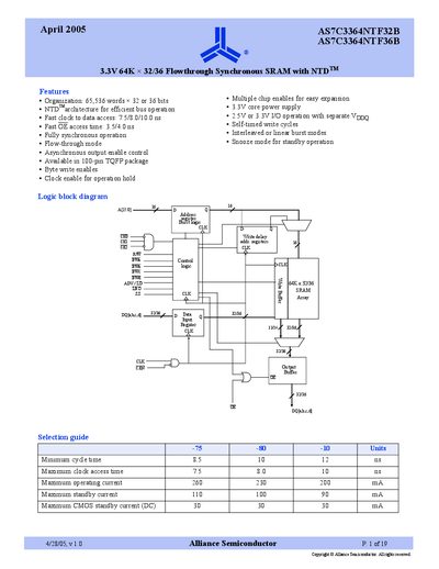
The AS7C3364NTF32B and AS7C3364NTF36B are 2 Mbit CMOS synchronous SRAMs organized as 65,536 words × 32 or 36 bits. They feature the No Turnaround Delay (NTD) architecture, fast clock‑to‑data access (7.5‑10 ns), and optional snooze mode for low‑power standby.
The devices operate from a 3.3 V core supply (VDD = 3.3 V + 0.165 V) with separate I/O supplies of 3.3 V or 2.5 V. They are offered in a 100‑pin TQFP package and support multiple chip‑enable pins, byte‑write enables, and burst‑mode operation.
| Organization | 65,536 words × 32 or 36 bits |
|---|---|
| Core supply voltage (VDD) | 3.3 V + 0.165 V |
| I/O supply voltage (VDDQ) | 3.3 V + 0.165 V for 3.3 V VO, 2.5 V + 0.125 V for 2.5 V VO |
| Package | 100‑pin TQFP |
| Clock‑to‑data access time | 7.5 ns / 8.0 ns / 10.0 ns |
| OE access time | 3.5 ns / 4.0 ns |
| Maximum operating current | 260 mA (32‑bit) / 230 mA (36‑bit) |
| Maximum standby current | 110 mA (32‑bit) / 100 mA (36‑bit) |
| Snooze mode standby current | 30 mA |
NTD stands for No Turnaround Delay, a trademark of Alliance Semiconductor.
The SRAM is supplied in a 100‑pin TQFP package.
The core supply voltage is 3.3 V ± 5 % (VDD = 3.3 V + 0.165 V).
The fastest clock‑to‑data access time is 7.5 ns, with options up to 10 ns.