
The ASM5P2309A / ASM5P2305A 3.3V Zero Delay Buffer is a high performance clock buffer used to distribute high speed clocks on CPU and PCI busses. It has zero input - output propagation delay, multiple low-jitter outputs and less than 250ps output - output jitter.
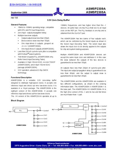
This document describes the ASM5P2309A and ASM5P2305A, which are 3.3V zero-delay buffers designed to distribute high-speed clocks with minimal propagation delay. The ASM5P2309A accepts one reference input and drives nine low-skew outputs, while the ASM5P2305A drives five outputs. Both devices utilize an on-chip PLL that locks to an input clock on the REF pin.
| Operating Frequency Range | 15MHz to 133MHz |
|---|---|
| Supply Voltage | 3.0V to 3.6V |
| Operating Temperature (Commercial) | 0°C to +70°C |
| Output-to-Output Skew | Less than 250ps |
| Device-to-Device Skew | Less than 700ps |
| Cycle-to-Cycle Jitter | Less than 200ps |
The devices support an operating range from 15MHz to 133MHz.
The devices operate at 3.3V, with a specified range of 3.0V to 3.6V.