
This datasheet introduces the ASM5P23S04A 3.3V zero-delay buffer, which has multiple configurations to meet the needs of different application scenarios. The device has zero input-output propagation delay, output-output skew less than 200ps, device-device skew less than 500ps, and can be used in PC, workstation, data communication, telecommunications and other high-performance applications.
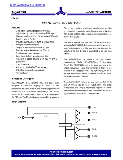
The ASM5P23S04A is a versatile, 3.3V zero-delay buffer designed to distribute high-speed clocks in PC, workstation, datacom, telecom and other high-performance applications. It features an on-chip PLL that locks to an input clock presented on the REF pin, with feedback driven to the FBK pin.
The device is available in multiple configurations including base parts (-1), high-drive versions (-1H, -5H), and frequency divider variants (-2). It offers two banks of outputs with guaranteed output-to-output skew less than 200 ps and device-to-device skew less than 500 ps when all outputs are equally loaded.
| Supply Voltage | 3.0 V to 3.6 V |
|---|---|
| Operating Temperature (Commercial) | 0 °C to 70 °C |
| Input Frequency Range | 10 MHz to 133 MHz |
| Output-to-Output Skew | Less than 200 ps |
| Device-to-Device Skew | Less than 500 ps |
| Package Type | 8-pin SOIC |
The maximum output frequency is 133.3 MHz when using a 20-pF load.
The delay is adjustable by varying the capacitive load on the FBK input relative to the other outputs.
The maximum supply voltage is 3.6 V.