
This file introduces M36L0T7050T2, M36L0T7050B2 two 128 Mbit (Multiple Bank, Multi-Level, Burst) Flash memory and 32 Mbit (2Mb x16) PSRAM, Multi-Chip Package features
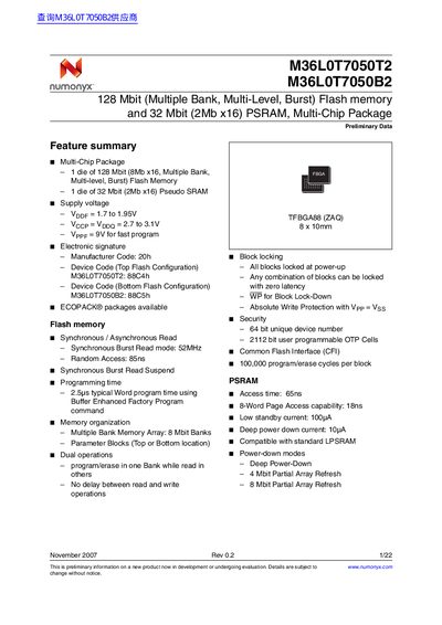
The M36L0T7050T2 and M36L0T7050B2 devices are offered as a stacked TFBGA88 multi‑chip package that integrates a 128‑Mbit multiple‑bank flash memory and a 32‑Mbit pseudo‑SRAM. The document describes the functional operation of both memory components, their pin assignments, and recommended operating conditions.
Key specifications include supply voltage ranges, read/write timing, power‑down modes, and endurance. The package is supplied with all bits erased and is intended for use in applications that require both non‑volatile flash storage and fast SRAM access within a single footprint.
| Flash memory capacity | 128 Mbit (8 Mb × 16) |
|---|---|
| PSRAM capacity | 32 Mbit (2 Mb × 16) |
| Flash programming supply voltage (Vppe) | 1.7 V to 1.95 V |
| Flash core supply voltage (Voce/Vppg) | 2.7 V to 3.1 V |
| Fast program voltage (Vppr) | 9 V |
| Synchronous burst read speed | 52 MHz |
| Random access read time | 85 ns |
| PSRAM access time | 65 ns |
| PSRAM 8‑word page access time | 18 ns |
| PSRAM standby current | 100 µA |
| PSRAM deep power‑down current | 10 µA |
| Program/erase endurance per block | 100 000 cycles |
| Number of flash memory banks | 8 Mbit banks |
The flash programming supply voltage (Vppe) is specified as 1.7 V to 1.95 V.
The flash memory is organized into eight 8‑Mbit banks.
The flash supports a synchronous burst read mode up to 52 MHz.
The PSRAM has a low standby current of 100 µA.