
The M25P10-A is a 1Mbit serial Flash memory with features like 2.3 to 3.6V single supply voltage, 50MHz clock rate (maximum), deep power-down mode 1µA (typical), JEDEC standard two-byte signature (2011h), RES instruction, one-byte signature (10h), more than 20 years' data retention etc.
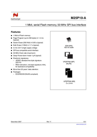
The handbook describes the M25P10-A 1 Mbit (128 Kbit × 8) serial Flash memory, its organization into four 256‑Kbit sectors and 512 pages, and its advanced write‑protection mechanisms. It lists key features such as a 50 MHz SPI‑compatible bus, 2.3‑3.6 V supply range, and low power‑down current.
Signal descriptions for the SPI interface (CS, CLK, DI, DO, HOLD, WP) are given, along with timing diagrams, package mechanical data for SO8, VFQFPN8 and UFDFPN8 options, and detailed electrical characteristics. Revision history and legal notices conclude the document.
| Memory capacity | 1 Mbit (128 Kbit × 8) |
|---|---|
| Supply voltage | 2.3 V to 3.6 V |
| Maximum SPI clock rate | 50 MHz |
| Page program time (256 bytes) | 1.4 ms (typical) |
| Sector erase time (256 Kbit) | 0.65 s (typical) |
The device supports up to a 50 MHz SPI clock rate.
The memory is organized as four sectors, each 256 Kbit.
A page program operation takes about 1.4 ms (typical).
The M25P10‑A operates from 2.3 V to 3.6 V single supply.