
AS7C252MFT18A is a 2.5V 32 Mb Synchronous SRAM with the following features: Organization: 2,097152 words × 18 bits, Fast clock to data access time: 7.5/8.5/10 ns, Fast OE access time: 3.5/4.0 ns, Fully synchronous flow-through operation, Asynchronous output enable control, Available in 100-pin TQFP package, Individual byte write and global write, Multiple chip enables for easy expansion, 2.5V core power supply, Linear or interleaved burst control, Snooze mode for reduced power-standby, Common data inputs and data outputs.
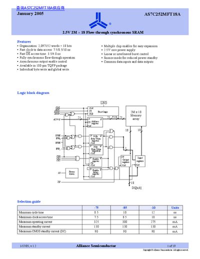
The AS7C252MFT18A is a high‑performance 32‑Mbit CMOS synchronous SRAM organized as 2,097,152 words × 18 bits. It offers fast clock‑to‑data access times of 7.5 ns, 8.5 ns or 10 ns and an asynchronous output‑enable access time of 3.5 ns to 4.0 ns. The device supports flow‑through burst operation, individual byte write, global write, multiple chip enables, and a low‑power snooze mode.
The SRAM is supplied from a 2.5 V core voltage (VDD) with I/O voltage (VDDQ) of 2.5 V + 0.125 V, and is available in a 100‑pin TQFP package. Detailed electrical ratings, timing diagrams, pin assignments, and truth tables are provided for design integration.
| Organization | 2,097,152 words × 18 bits |
|---|---|
| Core supply voltage (VDD) | 2.5 V + 0.125 V |
| I/O supply voltage (VDDQ) | 2.5 V + 0.125 V |
| Clock access time | 7.5 ns / 8.5 ns / 10 ns |
| OE access time | 3.5 ns / 4.0 ns |
| Package | 100‑pin TQFP |
| Maximum operating current | 325 mA |
| Maximum standby current | 130 mA |
| Maximum CMOS standby current (DC) | 90 mA |
| Input voltage (Vpp) range | 2.375 V – 2.625 V |
| I/O voltage (Vppe) range | 2.375 V – 2.625 V |
| Storage temperature range | -65 °C to +150 °C |
| Temperature under bias range | -65 °C to +135 °C |
The core supply voltage (VDD) is 2.5 V + 0.125 V.
It is offered in a 100‑pin TQFP package.
Maximum operating current is 325 mA, and maximum standby current is 130 mA.
The device provides clock‑to‑data access times of 7.5 ns, 8.5 ns or 10 ns.