
The ASM3P623S00A/B/C/D/E/F is a high performance, low jitter clock buffer with zero input-output propagation delay, output skew less than 250ps, device-device skew less than 700ps.
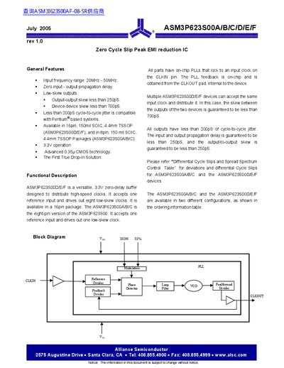
The ASM3P623S00 family is a 3.3 V zero‑delay buffer designed to distribute high‑speed clocks with very low skew and jitter. Variants are offered in 8‑pin and 16‑pin packages, supporting up to eight low‑skew clock outputs.
The document provides functional descriptions, pin configurations, electrical characteristics, absolute maximum ratings, package dimensions, and ordering information for all device variants.
| Input frequency range | 20 MHz – SOM Hz |
|---|---|
| Device‑to‑device skew | < 700 ps |
| Cycle‑to‑cycle jitter | < 200 ps |
| Supply voltage (VDD) | 3.0 V – 3.6 V |
| Operating temperature | 0 °C – 70 °C |
| Maximum storage temperature | -65 °C – +150 °C |
| Maximum soldering temperature (10 s) | 260 °C |
The devices operate over an input frequency range of 20 MHz to SOM Hz.
The part is specified for a 3.0 V to 3.6 V supply.
All outputs have less than 200 ps of cycle‑to‑cycle jitter.