
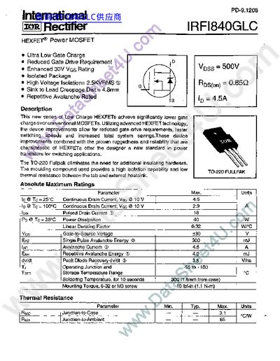
The IRFI840GLC is a low‑gate‑charge HEXFET power MOSFET designed for switching applications. It offers reduced gate drive requirements, fast switching speeds, and high voltage isolation up to 2.5 kV RMS. The device is supplied in a TO‑220 FullPak package that eliminates the need for additional insulating hardware.
The document lists absolute maximum ratings, electrical characteristics, capacitance data, and package dimensions. It includes typical output and transfer characteristics, thermal response curves, and detailed appendix sections covering test circuits, lead assignments, and part marking information.
| Gate‑to‑Source Voltage (Vgs) Rating | +30 V |
|---|---|
| Continuous Drain Current (Id) @ 25 °C | 45 A |
| Power Dissipation (Pd) | 40 W |
| Drain‑to‑Source Breakdown Voltage (Vds) | 500 V |
| On‑Resistance (Rds(on)) | 0.85 Ω (typ) |
| Total Gate Charge (Qg) | 2 nC |
| Input Capacitance (Cgs) | 1100 pF |
| Output Capacitance (Coss) | 170 pF |
The device is rated for a drain‑to‑source breakdown voltage of 500 V.
It can conduct up to 45 A continuously at 25 °C.
The MOSFET is supplied in a TO‑220 FullPak package.
The maximum gate‑to‑source voltage rating is +30 V.