
This PDF file is an introduction document about IDT49FCT805BT/CT and IDT49FCT806BT/CT products. It mainly introduces the features and characteristics of the products, including 0.5 micron CMOS process, low jitter, low power consumption, TTL compatible inputs and outputs, high drive, two independent output circuits, anti-static electricity and so on
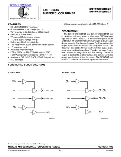
The IDT49FCT805BT/CT (non‑inverting) and IDT49FCT806BT/CT (inverting) are fast CMOS buffer/clock driver integrated circuits built on 0.5 µm technology. They feature low output skew (< 500 ps), TTL‑compatible inputs and outputs, high drive capability (‑32 mA IoH, 48 mA IOL), and a heartbeat monitor output for diagnostics.
The datasheet provides detailed pin configurations, electrical characteristics, switching parameters, test circuits, and ordering information. It lists available packages (DIP, SOIC, SSOP, QSOP, Cerpack, LCC), temperature ranges (commercial –55 °C to +70 °C, military –55 °C to +125 °C), and ESD protection (> 2000 V per MIL‑STD‑883).
| Technology node | 0.5 µm CMOS |
|---|---|
| Maximum output skew | < 500 ps |
| Drive current (high side) | -32 mA IoH |
| Drive current (low side) | 48 mA IOL |
| ESD rating | > 2000 V (MIL‑STD‑883 Method 3015) |
| Input HIGH level (VIH) | 2.0 V |
| Input LOW level (VIL) | 0.8 V |
| Commercial temperature range | -55 °C to +70 °C |
| Military temperature range | -55 °C to +125 °C |
The devices are rated for ESD protection greater than 2000 V per MIL‑STD‑883 Method 3015.
They are offered in DIP, SOIC, SSOP, QSOP, Cerpack, and LCC packages.
The high‑side drive current is –32 mA (IoH) and the low‑side drive current is 48 mA (IOL).
The devices guarantee a maximum output skew of less than 500 ps.