
The FCT3805/A is a 3.3 volt, non-inverting clock driver built using advanced dual metal CMOS technology. The device consists of two banks of drivers, each with a 1:5 fanout and its own output enable control. The device has a "heartbeat" monitor for diagnostics and PLL driving. The MON output is identical to all other outputs and complies with the output specifications in this document. The FCT3805/A offers low capacitance inputs with hysteresis. The FCT3805/A is designed for high speed clock distribution where signal quality and skew are critical. The FCT 3805 also allows single point-to-point transmission line driving in applications such as address distribution, where one signal must be distributed to multiple receivers with low skew and high signal quality.
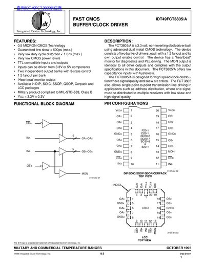
The IDT49FCT3805/A is a fast CMOS buffer/clock driver built on 0.5 µm technology. It provides guaranteed low skew (< 500 ps), very low duty‑cycle distortion (< 1.0 ns), TTL‑compatible inputs that can be driven from 3.3 V or 5 V, and two independent 3‑state output banks with 1:5 fan‑out per bank. The device includes a heartbeat monitor output for diagnostics and is available in a wide range of packages.
Electrical specifications cover input‑high and low thresholds, output drive capabilities, propagation delays, and power‑supply characteristics across commercial (0 °C to +70 °C) and military (‑55 °C to +125 °C) temperature ranges. Ordering information lists the supported packages such as DIP, SOIC, SSOP, QSOP, Cerpack and LCC, and indicates compliance with MIL‑STD‑883 Class B.
| Technology | 0.5 µm CMOS |
|---|---|
| Maximum Skew | < 500 ps (max) |
| Duty‑Cycle Distortion | < 1.0 ns (max) |
| Supply Voltage (VCC) | 3.3 V ±0.3 V |
| Output Fan‑out | 1:5 per bank |
The device guarantees a low skew of less than 500 ps (max).
It is offered in DIP, SOIC, SSOP, QSOP, Cerpack and LCC packages.