
AO4806 is a dual N-channel enhancement mode field effect transistor produced by Alpha & Omega Semiconductor, Ltd. It features excellent RDS(ON) and low gate charge. This device is suitable for use as a uni-directional or bi-directional load switch, facilitated by its common-drain configuration. The maximum VDS of AO4806 is 20V and the maximum VGS is 12V.
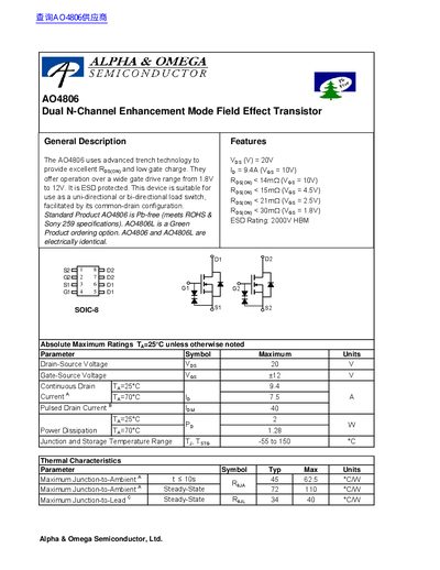
The AO4806 is a dual N‑channel enhancement mode field‑effect transistor that uses trench technology to achieve low on‑resistance and low gate charge. It operates over a gate‑drive range of 1.8 V to 12 V and is ESD protected, making it suitable for uni‑directional or bi‑directional load‑switch applications.
The datasheet lists absolute maximum ratings, thermal characteristics, and detailed electrical parameters such as drain‑source voltage, gate‑source voltage, continuous and pulsed drain currents, and capacitances. Typical curves illustrate on‑resistance versus drain current, transfer characteristics, and gate‑charge behavior.
| Gate‑Source Voltage (Vgs) | +12 V |
|---|---|
| Drain‑Source Voltage (Vds) | 20 V |
| Continuous Drain Current (Id) @ 25 °C | 9.4 A |
| Pulsed Drain Current | 40 A |
| ESD Rating | 2000 V HBM |
| Total Gate Charge (Qg) | 17.9 nC |
| Input Capacitance (Ciss) | 1810 pF |
| Output Capacitance (Coss) | 232 pF |
| Power Dissipation (PD) | 1.28 W |
| Operating Temperature Range | -55 °C to 150 °C |
The AO4806 can handle a continuous drain current of 9.4 A at 25 °C.
The device is rated for 2000 V HBM ESD protection.
The drain‑source voltage is limited to 20 V and the gate‑source voltage to +12 V.
The total gate charge is specified as 17.9 nC.