
The AO4414A is a N-channel enhancement mode field effect transistor with the following features: VDS (V) = 30V ID = 8.5A (VGS = 10V), RDS (ON) <26mΩ (VGS = 10V), RDS (ON) <40mΩ (VGS = 4.5V).
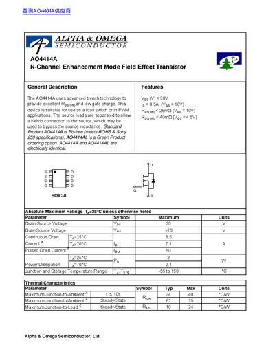
The AO4414A is an N‑Channel enhancement mode MOSFET featuring a 30 V drain‑source breakdown voltage and an on‑state resistance as low as 26 mΩ at VGS = 10 V. It is designed for load‑switch and PWM applications and includes a Kelvin source connection to reduce source inductance.
The datasheet lists detailed static, dynamic and switching parameters, thermal resistance values, and typical characteristic curves. It also notes that the device is Pb‑free, RoHS compliant, and intended for consumer‑market use only; it is not authorized for life‑support systems.
| Drain‑Source Breakdown Voltage (VDS) | 30 V |
|---|---|
| Continuous Drain Current (ID) | 8.5 A |
| On‑State Resistance (RDS(ON)) | < 26 mΩ @ VGS=10 V |
| Gate Threshold Voltage (VGS(th)) | Typical 1 V |
| Gate Charge (Qg) @ 10 V | 11.3 nC |
| Thermal Resistance Junction‑to‑Ambient (RθJA) | 40 °C/W |
The device is rated for a maximum drain‑source voltage of 30 V.
It can conduct up to 8.5 A continuously.
Yes, the AO4414A is Pb‑free and meets RoHS specifications.
The on‑state resistance is less than 26 mΩ at VGS = 10 V.