
This document is the functional description of SY10/100E241 8-bit scannable register, including timing diagram and pin definition, and details its data input, output, register operation and other characteristics
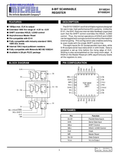
The SY10E241 and SY100E241 are 8‑bit shiftable registers designed for high‑performance ECL systems. They feature internal data feedback so that the SHIFT control overrides HOLD and /LOAD, allowing single‑line control of scan mode. Parallel inputs D0‑D7 and a serial input S‑IN are provided, with data shifting on the rising edge of the clock. A high Master Reset pin asynchronously clears all registers.
The datasheet lists the device's electrical characteristics, including a maximum shift frequency of 700‑900 MHz, propagation delays of 625‑975 ps, input high current of 150 µA, and power‑supply current of 125‑150 mA. The part is supplied in a 28‑lead PLCC (J28‑1) package and operates with a VEE range of –4.2 V to –5.5 V.