
This document is a specification for a specific product, describing the pin definitions and functional characteristics of the product.
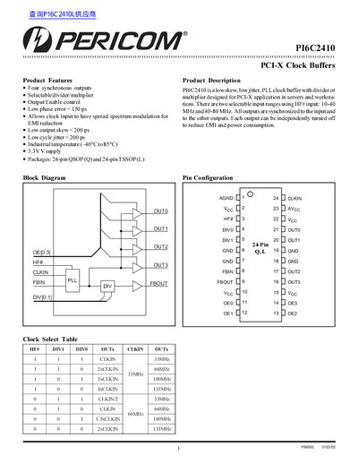
The Pericom PI6C2410 is a low-skew, low-jitter Phase Locked Loop (PLL) clock buffer featuring selectable divider or multiplier functionality. It is specifically designed for PCI-X applications in servers and workstations, supporting input ranges of 10-40 MHz and 40-80 MHz via the HF# pin selection.
| Input Voltage Range (Low) | 0.8 V |
|---|---|
| Input Voltage Range (High) | 2.0 V |
| Supply Voltage (Vcc, AVcc) | 3.0 V to 3.6 V |
| Output Skew (Max) | < 200 ps |
| Cycle Jitter (Max) | < 200 ps |
The device supports two selectable input ranges: 10-40 MHz and 40-80 MHz, selected using the HF# input.
The part is available in a 24-pin QSOP (Q) package and a 24-pin TSSOP (L) package.
The maximum supply current (Idd_133) is 60 mA when the load capacitance is 15pF.