
CD4071B, CD4072B, and CD4075B OR gates provide the system designer with direct implementation of the positive-logic OR function and supplement the existing family of CMOS gates. The CD4071B, CD4072B, and CD4075B types are supplied in 14-lead hermetic dual-in-line ceramic packages (F3A suffix), 14-lead dual-in-line plastic packages (E suffix), 14-lead small-outline packages (M, MT, M96, and NSR suffixes), and 14-lead thin shrink small-outline packages (PW and PWR suffixes).
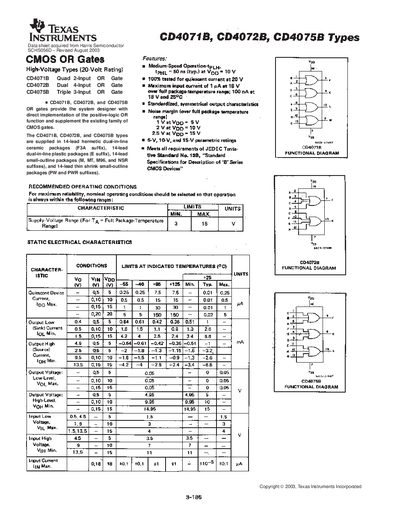
The CD4071B, CD4072B and CD4075B are high‑voltage CMOS OR gate devices offered in a variety of 14‑lead packages. They provide medium‑speed operation with typical propagation delay of 60 ns at a 10 V supply and feature low quiescent current.
The document includes recommended operating conditions, absolute‑maximum ratings, electrical characteristics, functional diagrams, package options, mechanical drawings and regulatory notices. Package options cover PDIP, SOIC, TSSOP and small‑outline packages with RoHS‑compliant finishes.
| Input Voltage Range (all inputs) | -0.8 V to Vpp + 0.5 V |
|---|---|
| Typical Propagation Delay | 60 ns at Vpp = 10 V |
Typical propagation delay is 60 ns when powered at 10 V.
Inputs may be driven from –0.8 V up to Vpp + 0.5 V.