
SN65LVDS33, SN65LVDT33, SN65LVDS34, and SN65LVDT34 are high-speed differential receivers. They operate with a single 3.3V supply and have a signaling rate of up to 400Mbps and a data transfer rate of 200Mxfr/s. They have a -4V to 5V common-mode input voltage range, with differential input thresholds <±50mV and 50mV of hysteresis over the entire common-mode input voltage range. The LVDT products have integrated 110Ω line termination resistors. They comply with TIA/EIA-644 (LVDS) and have active failsafe to ensure a high-level output with no input. The bus-pin ESD protection exceeds 15kV HBM. The inputs remain high-impedance on power down and are 5V TTL tolerant. They are pin-compatible with the AM26LS32, SN65LVDS32B, µA9637, and SN65LVDS9637B, and are available in TSSOP packaging.
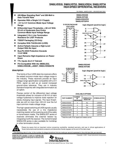
The SN65LVDS33, SN65LVDT33, SN65LVDS34 and SN65LVDT34 are high‑speed differential receivers that operate from a single 3.3 V supply and support a wide common‑mode input voltage range. They include integrated line termination options, an active failsafe circuit, and can tolerate high electrostatic discharge levels.
The document provides electrical characteristics, absolute maximum ratings, switching performance, mechanical dimensions, and warranty notices for these devices, along with test circuit diagrams and measurement procedures.
| Supply voltage (Voc) | 3.3 V – 3.6 V |
|---|---|
| High‑level input voltage (VjH) | 2 V – 5 V |
| Low‑level input voltage (VL) | 0 V – 0.8 V |
| Operating temperature range | -40 °C – 85 °C |
| Propagation delay (low‑to‑high) | 2.5 ns – 6 ns |
The receivers can withstand +15 kV human‑body model (HBM) and +600 V machine model (MM) discharges to the input pins.
The recommended supply voltage (Voc) is 3.3 V to 3.6 V.
The devices are specified to operate from –40 °C to 85 °C.
Yes, they include a patent‑pending active failsafe circuit that provides a high‑level output within 600 ns after loss of the input signal.