
This data sheet mainly introduces the features and characteristics of CD54HC32, CD54HCT32, CD74HC32, CD74HCT32, including propagation delay, fanout, operating temperature range, input output logic compatibility, etc.
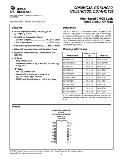
The CD54HC32, CD74HC32, CD54HCT32 and CD74HCT32 are quad 2‑input OR gate CMOS logic devices that combine high‑speed operation with low power consumption. They are pin‑compatible with standard LS logic families and can drive up to ten LSTTL loads.
The document provides absolute maximum ratings, operating conditions, detailed DC electrical specifications, switching performance, and packaging options (CDIP, PDIP, SOIC). Ordering information, package material details, mechanical drawings, and legal notices are also included.
| Typical Propagation Delay | 7 ns at VCC = 5 V |
|---|---|
| Fanout (LSTTL loads) | 10 loads |
| Operating Temperature Range | -55 °C to 125 °C |
| Input High Voltage (VIH) typical | 4.5 V |
| Input Low Voltage (VIL) typical | 0.8 V |
| Output Low Voltage (VOL) typical | 0.1 V |
The typical propagation delay is 7 ns when VCC is 5 V.
Each device can drive up to ten LSTTL loads.
The devices are rated for –55 °C to 125 °C.