
The MAX1134/MAX1135 are 150ksps, 16-bit ADCs. These serially interfaced ADCs connect directly to SPI™, QSPI™, and MICROWIRE™ devices without external logic. They combine an input scaling network, internal track/hold (T/H), clock, and three general-purpose digital output pins (for external multiplexer or PGA control) in a 20-pin SSOP package. The excellent dynamic performance (THD ≥ 90dB), high speed (150ksps in bipolar mode), and low power (8.0mA) of these ADCs make them ideal for applications such as industrial process control, instrumentation, and medical applications. The MAX1134 accepts input signals of 0 to +6V (unipo- lar) or ±6V (bipolar), while the MAX1135 accepts input signals of 0 to +2.048V (unipolar) or ±2.048V (bipolar). Operating from a single 3.135V to 3.465V analog and digital supply, power-down modes reduce current con- sumption to 0.15mA at 10ksps and further reduce sup- ply current to less than 20µA at slower data rates. A serial strobe output (SSTRB) allows direct connection to the TMS320 family digital-signal processors. The MAX1134/MAX1135 user can select either the internal clock or an external serial-interface clock for the ADC to perform analog-to-digital conversions. The MAX1134/MAX1135 feature internal calibration cir- cuitry to correct linearity and offset errors. On-demand calibration allows the user to optimize performance. Three user-programmable logic outputs are provided for the control of an 8-channel mux or PGA.
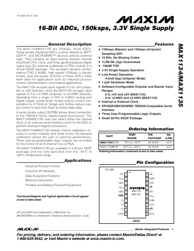
The MAX1134 and MAX1135 are 16‑bit successive‑approximation ADCs capable of 150 ksps in bipolar mode and 125 ksps in unipolar mode. They operate from a single 3.3 V supply and include an input scaling network, internal track‑and‑hold, a clock generator, three user‑programmable digital outputs, and on‑demand calibration circuitry. The devices are offered in a 20‑pin SSOP package and are specified for –40 °C to +85 °C operation.
The datasheet provides absolute maximum ratings, detailed electrical and timing characteristics, pin descriptions, and functional block diagrams. It also explains the digital interface (SPI/QSPI/MICROWIRE), shutdown behavior, and how to configure input ranges and programmable outputs via the control byte.
| Resolution | 16 bits |
|---|---|
| Maximum Sampling Rate (bipolar) | 150 ksps |
| Supply Voltage (AVDD/DVDD) | 3.135 V to 3.465 V |
| Typical Power Consumption | 8.0 mA |
| Shutdown Current (10 ksps) | 0.15 mA |
| Shutdown Current (slow rates) | <20 µA |
| Input Range (MAX1134) | 0 V to +6 V (unipolar) or ±6 V (bipolar) |
| Input Range (MAX1135) | 0 V to +2.048 V (unipolar) or ±2.048 V (bipolar) |
| User‑Programmable Digital Outputs | 3 (P0, P1, P2) |
The devices can sample at up to 150 ksps in bipolar mode (125 ksps in unipolar mode).
Three push‑pull CMOS outputs (P0, P1, P2) are available for user programming.
Both analog and digital supplies must be between 3.135 V and 3.465 V.