
The MAX9176/MAX9177 are 670MHz, low-jitter, low-skew 2:1 multiplexers ideal for protection switching, loopback, and clock distribution. The devices feature ultra-low 68ps peak-to-peak deterministic jitter that ensures reliable operation in high-speed links that are highly sensitive to timing errors. The MAX9176 has fail-safe LVDS inputs and an LVDS output. The MAX9177 has “anything” differential inputs (CML/LVDS/LVPECL) and an LVDS output. The output can be put into high impedance using the power-down input. The MAX9176 features fail-safe circuits that drive the output high when a selected input is open, undriven and shorted, or undriven and terminated. The MAX9177 has bias circuits that force the output high when a selected input is open. The mux select and power-down inputs are compatible with standard LVTTL/ LVCMOS logic. The select and power-down inputs tolerate undershoot of -1V and overshoot of VCC + 1V. The MAX9176/ MAX9177 are available in 10-pin µMAX and 10-lead thin QFN packages, and operate from a single 3.3V supply over the -40°C to +85°C temperature range.
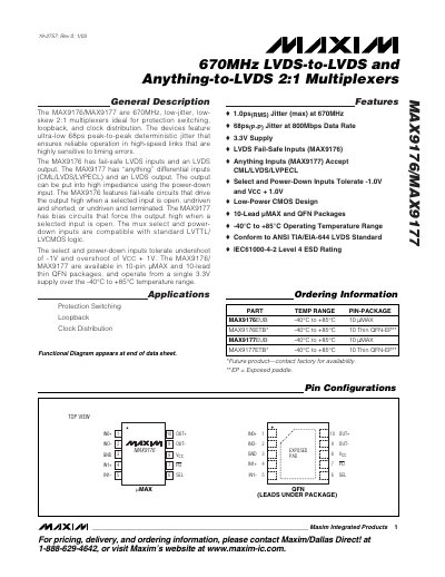
The MAX9176 and MAX9177 are 670 MHz, low‑jitter, low‑skew 2:1 multiplexers designed for protection switching, loopback, and clock distribution. The MAX9176 provides fail‑safe LVDS inputs and an LVDS output, while the MAX9177 accepts CML, LVDS, or LVPECL differential inputs and also outputs LVDS.
Both devices operate from a single 3.3 V supply over a temperature range of –40 °C to +85 °C and are available in 10‑pin µMAX and 10‑lead thin QFN packages. The datasheet includes electrical characteristics, timing parameters, layout recommendations, and package drawings.
| Operating Temperature Range | -40 °C to +85 °C |
|---|---|
| Supply Voltage | 3.3 V |
| Input Types (MAX9177) | CML, LVDS, LVPECL |
The MAX9177 accepts CML, LVDS, and LVPECL differential inputs.
The output can be put into high‑impedance by using the power‑down input.
The devices operate from a single 3.3 V supply (3.0 V to 3.6 V allowed).