
The MAX9392/MAX9393 dual 2 x 2 crosspoint switches perform high-speed, low-power, and low-noise signal distribution. The MAX9392/MAX9393 multiplex one of two differential input pairs to either or both low-voltage differential signaling (LVDS) outputs for each channel. Independent enable inputs turn on or turn off each differential output pair. Four LVCMOS/LVTTL logic inputs (two per channel) control the internal connections between inputs and outputs. This flexibility allows for the following configurations: 2 x 2 crosspoint switch, 2:1 mux, 1:2 splitter, or dual repeater. This makes the MAX9392/MAX9393 ideal for protection switching in fault-tolerant systems, loopback switching for diagnostics, fanout buffering for clock/data distribution, and signal regeneration. Fail-safe circuitry forces the outputs to a differential low condition for undriven inputs or when the common-mode voltage exceeds the specified range. The MAX9392 provides high-level input fail-safe detection for LVDS, HSTL, and other GND-referenced differential inputs. The MAX9393 provides low-level input fail-safe detection for LVPECL, CML, and other VCC-referenced differential inputs. Ultra-low 98ps(P-P) (max) pseudorandom bit sequence (PRBS) jitter ensures reliable communications in high-speed links that are highly sensitive to timing error, especially those incorporating clock-and-data recovery, or serializers and deserializers. The high-speed switching performance guarantees 1.5 Gbps communication rate.
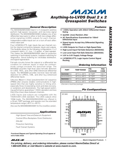
The MAX9392 and MAX9393 are dual 2 × 2 crosspoint switches that provide high‑speed, low‑power signal distribution for LVDS, HSTL, LVPECL and CML differential interfaces. They support configurable modes such as 2 × 2 switching, 2:1 multiplexing, 1:2 splitting and dual repeater operation, making them suitable for fault‑tolerant protection switching and clock/data fan‑out applications.
The devices are offered in a 32‑pin TQFP package, operate from –40 °C to +85 °C, and support up to 1.5 GHz data rates. Detailed electrical characteristics, pin descriptions, and layout recommendations are provided to aid board designers in implementing reliable high‑speed LVDS links.
| Supply Voltage Range | 3.0 V to 3.6 V |
|---|---|
| Operating Temperature Range | -40 °C to +85 °C |
| Package | 32‑pin TQFP |
| Maximum Data Rate | 1.5 GHz |
| LVDS Output Load | 100 Ω termination |
The devices operate from 3.0 V to 3.6 V supply voltage.
They support up to 1.5 GHz operation.
Both devices are supplied in a 32‑pin TQFP package.
A 100 Ω resistor should be placed between each LVDS differential output pair.