
The MAX9312/MAX9314 are low skew, dual 1-to-5 differential drivers designed for clock and data distribution. They feature low part-to-part skew and output-to-output skew, making them ideal for clock and data distribution across a backplane or a board. They operate over a +2.25V to +3.8V supply range for interfacing to differential HSTL and LVPECL signals, allowing high-performance clock or data distribution in systems with a nominal +2.5V or +3.3V supply. For differential LVECL operation, they operate from a -2.25V to -3.8V supply. They are offered in an industry-standard 32-pin 7mm x 7mm LQFP package and a space-saving 32-pin 5mm x 5mm TQFN package.
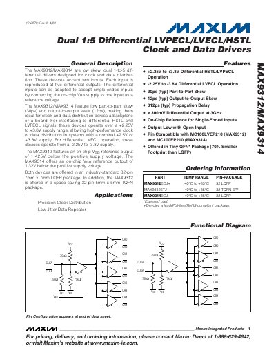
The MAX9312 and MAX9314 are low‑skew, dual 1‑to‑5 differential drivers designed for clock and data distribution. They accept two inputs and reproduce each on five differential outputs, supporting LVPECL, LVECL, and HSTL signal standards. The devices operate from a +2.25 V to +3.8 V supply for LVPECL/HSTL and from –2.25 V to –3.8 V for LVECL, with on‑chip VBB reference outputs for single‑ended operation.
The datasheet provides absolute maximum ratings, DC and AC electrical characteristics, typical operating curves, pin descriptions, and package options (32‑pin LQFP and 32‑pin TQFN). It also includes application notes on supply bypassing, trace impedance, and output termination for optimal performance. This manual is written in Chinese.
| Supply Voltage Range (LVPECL/HSTL) | +2.25 V to +3.8 V |
|---|---|
| Supply Voltage Range (LVECL) | -2.25 V to -3.8 V |
| Part‑to‑Part Skew (typ) | 30 ps |
| Output‑to‑Output Skew (typ) | 12 ps |
| Propagation Delay (typ) | 312 ps |
| Differential Output Voltage (min) | ≥300 mV at 3 GHz |
| On‑Chip VBB Reference (MAX9312) | VCC‑1.425 V |
| On‑Chip VBB Reference (MAX9314) | VCC‑1.32 V |
| Package Options (MAX9312) | 32‑pin LQFP, 32‑pin TQFN |
Typical part‑to‑part skew is 30 ps.
The MAX9312 is available in a 32‑pin LQFP package and a 32‑pin TQFN package.
The MAX9314 provides an on‑chip VBB reference of VCC‑1.38 V.