
The MAX9311/MAX9313 are low-skew, 1-to-10 differential drivers designed for clock and data distribution. These devices allow selection between two inputs. The selected input is reproduced at 10 differential outputs. The differential inputs can be adapted to accept single- ended inputs by connecting the on-chip VBB supply to one input as a reference voltage. The MAX9311/MAX9313 feature low part-to-part skew (30ps) and output-to-output skew (12ps), making them ideal for clock and data distribution across a backplane or a board. For interfacing to differential HSTL and LVPECL signals, these devices operate over a +2.25V to +3.8V supply range, allowing high-performance clock or data distribution in systems with a nominal +2.5V or +3.3V supply. For differential LVECL operation, these devices operate from a -2.25V to -3.8V supply. The MAX9311 features an on-chip VBB reference output of 1.425V below the positive supply voltage. The MAX9313 offers an on-chip VBB reference output of 1.32V below the positive supply voltage. Both devices are offered in space-saving, 32-pin 5mm ✕ 5mm TQFP, 5mm x 5mm QFN, and industry-standard 32-pin 7mm x 7mm LQFP packages.
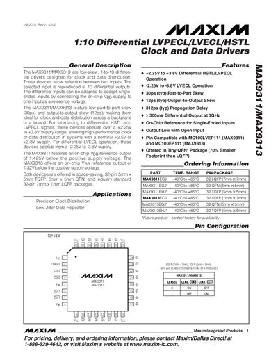
The MAX9311 and MAX9313 are low‑skew, 1‑to‑10 differential drivers intended for clock and data distribution in high‑speed digital systems. They support selectable LVPECL, LVECL, and HSTL signaling with supply ranges of +2.25 V to +3.8 V (positive) or –2.25 V to –3.8 V (negative) and provide on‑chip reference voltages for single‑ended operation.
The devices feature 10 differential outputs, a 2:1 input multiplexer controlled by a single‑ended CLKSEL pin, and specifications such as 30 ps typical part‑to‑part skew and 12 ps typical output‑to‑output skew. Package options include 32‑pin QFN, TQFP and LQFP formats with detailed pin descriptions and layout recommendations.
| Supply Voltage (LVPECL/HSTL) | +2.25 V to +3.8 V |
|---|---|
| Supply Voltage (LVECL) | -2.25 V to -3.8 V |
| Part‑to‑Part Skew (typ) | 30 ps |
| Output‑to‑Output Skew (typ) | 12 ps |
| Propagation Delay (typ) | 312 ps |
| Differential Output Voltage | >300 mV at 3 GHz |
| Number of Differential Outputs | 10 |
The typical part‑to‑part skew is 30 ps.
LVPECL operation requires a positive supply between +2.25 V and +3.8 V.
Each device provides ten differential outputs.
The typical output‑to‑output skew is 12 ps.