
The MAX9394/MAX9395 consist of a 2:1 multiplexer and a 1:2 demultiplexer with loopback. The multiplexer section (channel B) accepts two low-voltage differential signaling (LVDS) inputs and generates a single LVDS output. The demultiplexer section (channel A) accepts a single LVDS input and generates two parallel LVDS outputs. The MAX9394/MAX9395 feature a loopback mode that connects the input of channel A to the output of channel B and connects the selected input of channel B to the outputs of channel A. Three LVCMOS/LVTTL logic inputs control the internal connections between inputs and outputs, one for the multiplexer portion of channel B (BSEL), and the other two for loopback control of channels A and B (LB_SELA and LB_SELB). Independent enable inputs for each differential output pair provide additional flexibility. Fail-safe circuitry forces the outputs to a differential low condition for undriven inputs or when the common-mode voltage exceeds the specified range. The MAX9394 provides high-level input fail-safe detection for HSTL, LVDS, and other GND-referenced differential inputs. The MAX9395 provides low-level fail-safe detection for CML, LVPECL, and other VCC-referenced differential inputs. Ultra low 91psP-P (max) pseudorandom bit sequence (PRBS) jitter ensures reliable communications in high-speed links that are highly sensitive to timing error, especially those incorporating clock-and-data recovery, or serializers and deserializers.
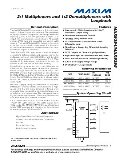
The MAX9394 and MAX9395 are high‑speed LVDS multiplexers/demultiplexers that provide a 2:1 multiplexing function on channel B and a 1:2 demultiplexing function on channel A, with independent loopback control. They support 1.5 GHz operation, 250 mV differential output swing, and include fail‑safe detection for both high‑ and low‑level inputs.
The devices are offered in a 32‑pin TQFP package, operate from –40 °C to +85 °C, and require a 3.0 V to 3.6 V supply. Detailed pin descriptions, electrical characteristics, and layout recommendations are provided to aid designers in high‑speed telecom and datacom applications.
| Supply Voltage Range | 3.0 V to 3.6 V |
|---|---|
| Operating Temperature Range | -40 °C to +85 °C |
| Package | 32‑pin TQFP |
| Differential Output Swing | 250 mV |
| Maximum Switching Frequency | 1.5 GHz |
| Input High Voltage (V_IH) | 2.0 VCC |
| LVDS Output Load | 100 Ω |
The devices operate from 3.0 V to 3.6 V.
They are rated for –40 °C to +85 °C.
Both parts are offered in a 32‑pin TQFP package.
They support up to 1.5 GHz operation.