
The CD4001B, CD4002B, and CD4025B types are supplied in 14-lead hermetic dual-in-line ceramic packages (F3A suffix), 14-lead dual-in-line plastic packages (E suffix), 14-lead small-outline packages (M, MT, M96, and NSR suffixes), and 14-lead thin shrink small-outline packages (PW and PWR suffixes).
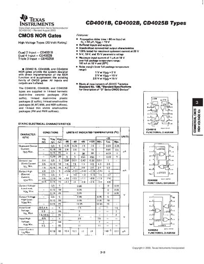
The CD4001B, CD4002B, and CD4025B are high‑voltage CMOS NOR gates offered in a variety of 14‑lead packages, including hermetic ceramic, plastic DIP, small‑outline (SO), and thin‑shrink SO packages. All inputs and outputs are buffered, providing standardized symmetrical output characteristics.
The document provides static and dynamic electrical characteristics, recommended operating conditions, and mechanical dimensions for each package type. It also includes a warranty notice and packaging status information for each device variant.
| Propagation delay time (typical) | 60 ns at CL = 50 pF, Vpp = 10 V |
|---|---|
| Input voltage range (all inputs) | -0.8 V to Vpp + 0.5 V |
| Maximum input current | 1 A at 18 V |
The typical propagation delay time is 60 ns when the load capacitance is 50 pF and Vpp is 10 V.
The CD4001B is offered in hermetic dual‑in‑line ceramic (F3A), plastic dual‑in‑line (E), small‑outline (M, MT, M96, NSR), and thin‑shrink small‑outline (PW, PWR) packages.
All inputs accept voltages from –0.8 V up to Vpp + 0.5 V.