
This datasheet provides detailed information on SN54HC21/74HC21, including function description, pin definition, internal connection, package dimension, ordering information, etc.
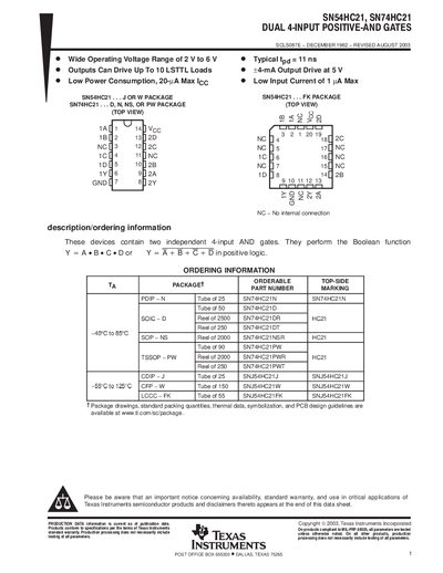
The SN54HC21 and SN74HC21 are dual 4‑input positive‑AND gate devices that implement the Boolean function Y = A·B·C·D. They operate with positive logic and are offered in a variety of packages such as PDIP, SOIC, TSSOP and more.
Key electrical characteristics include a wide supply voltage range of 2 V to 6 V, typical propagation delay of 11 ns, low power consumption (≈20 µA max) and low input current (≈1 µA max). The outputs can drive up to 10 LSTTL loads and provide up to +4 mA at 5 V. Detailed ordering information, package drawings, mechanical dimensions and an important notice about product warranties are also provided.
| Supply voltage range | 2 V to 6 V |
|---|---|
| Typical propagation delay | 11 ns |
| Output drive capability | Up to 10 LSTTL loads |
| Low power consumption | 20 µA max |
| Low input current | 1 µA max |
The devices operate from 2 V to 6 V.
Typical propagation delay is 11 ns.
Each output can drive up to 10 LSTTL loads.