
STP6NB90 is an advanced family of power MOSFETs with outstanding performances designed by STMicroelectronics using the latest high voltage MESH OVERLAY process. The new patent pending strip layout coupled with the Companys proprietary edge termination structure, gives the lowest RDS(on) per area, exceptional avalanche and dv/dt capabilities and unrivalled gate charge and switching characteristics. This product is suitable for high current, high speed switching, switch mode power supplies (SMPS), DC-AC converters for welding equipment and uninterruptible power supplies and motor drive applications.
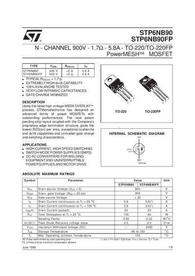
The document provides detailed specifications for the STP6NB90 and STP6NB90FP N‑channel power MOSFETs, including electrical ratings, thermal performance, and mechanical dimensions. It highlights the devices' high voltage capability (900 V), low on‑resistance, and robust avalanche characteristics.
Key sections cover description, applications, absolute maximum ratings, thermal data, electrical and switching characteristics, mechanical data, and thermal impedance, along with legal and copyright information.
| Drain‑source Voltage (VDS) max | 900 V |
|---|---|
| Gate‑source Voltage (VGS) max | 30 V |
| Continuous Drain Current @ 25 °C | 5.8 A |
| Continuous Drain Current @ 100 °C | 3.6 A |
| Pulsed Drain Current | 23 A |
| Total Dissipation @ 25 °C | 135 W |
| Typical On‑Resistance (RDS(on)) | 1.7 mΩ |
| Thermal Resistance Junction‑case | 1.08 °C/W |
| Thermal Resistance Junction‑ambient | 62.5 °C/W |
| Avalanche Current (repetitive) | 5.8 A |
| Single‑Pulse Avalanche Energy | 250 mJ |
| Maximum Operating Junction Temperature | 150 °C |
The maximum drain‑source voltage is 900 V.
The typical on‑resistance is 1.7 mΩ.
It can handle up to 5.8 A of continuous drain current at 25 °C.
The device is rated for a maximum junction temperature of 150 °C.