
74VHCT08A is an advanced high-speed CMOS QUAD 2-INPUT AND GATE fabricated with sub-micron silicon gate and double-layer metal wiring C2MOS technology. The internal circuit is composed of 2 stages including buffer output, which provides high noise immunity and stable output. Power down protection is provided on all inputs and outputs and 0 to 7V can be accepted on inputs with no regard to the supply voltage.
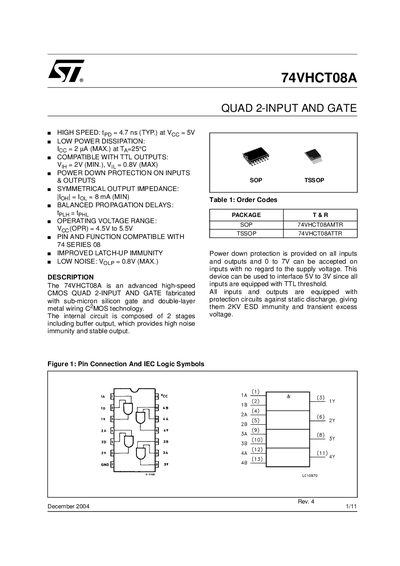
The 74VHCT08A is a high‑speed CMOS quad 2‑input AND gate with TTL‑compatible inputs and low power dissipation. It features power‑down protection on all pins, symmetrical output impedance, and balanced propagation delays.
The document provides pin descriptions, truth tables, absolute maximum ratings, recommended operating conditions, electrical and mechanical specifications, and revision history for the device.
| High speed propagation delay (tpp) | 4.7 ns (typ.) at Vcc=5V |
|---|---|
| Low power dissipation (Icc) | 2 µA (max) at Ta=25°C |
| Operating voltage range (Vcc) | 4.5 V to 5.5 V |
| Input high level voltage (VIH) | 2 V (min) |
| Input low level voltage (VIL) | 0.8 V (max) |
| Absolute maximum supply voltage (Voc) | -0.5 V to +7.0 V |
The device operates from 4.5 V to 5.5 V.
The supply voltage may not exceed –0.5 V to +7.0 V.
Typical propagation delay is about 4.7 ns at a 5 V supply.