
The TPS2041A through TPS2044A and TPS2051A through TPS2054A power-distribution switches are intended for applications where heavy capacitive loads and short circuits are likely to be encountered. Each switch is controlled by an independent logic enable input. Gate drive is provided by an internal charge pump designed to control the power-switch rise times and fall times to minimize current surges during switching. These devices limit the output current to a safe level when the output load exceeds the current-limit threshold or a short is present.
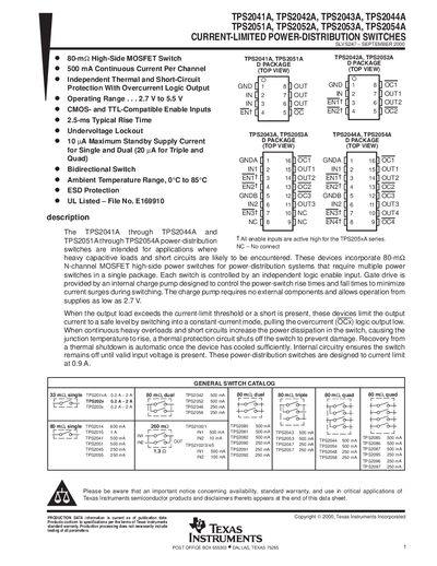
The TPS204x and TPS205x series are high‑side N‑channel MOSFET power‑distribution switches with built‑in current limiting, thermal protection and undervoltage lockout. Each channel is controlled by an independent enable input and includes an internal charge pump that allows operation from supplies as low as 2.7 V.
The devices provide up to 500 mA continuous current per channel, feature a typical 2.5 ms rise time, and incorporate dual‑threshold thermal trip circuitry that shuts off a faulty switch while keeping adjacent switches active. Detailed pin descriptions, functional block diagrams and package dimensions are included.
| Maximum continuous current per channel | 500 mA |
|---|---|
| Operating voltage range | 2.7 V to 5.5 V |
| Typical rise time | 2.5 ms |
| Maximum standby supply current | 10 A |
| On‑state resistance (RDS(on)) | 135 mΩ |
| Thermal trip temperature | ≈ 140 °C |
| Undervoltage lockout threshold | ≈ 2 V |
A logic low on the EN pin turns on the power switch for TPS2041A.
The driver’s typical rise time is 2.5 ms.
The internal charge pump operates from input voltages as low as 2.7 V.