
The CD4073B, CD4081B, and CD4082B types are supplied in 14-lead hermetic dual-in-line ceramic packages (F3A suffix), 14-lead dual-in-line plastic packages (E suffix), 14-lead small-outline packages (M, MT, M96, and NSR suffixes), and 14-lead thin shrink small-outline packages (PW and PWR suffixes).
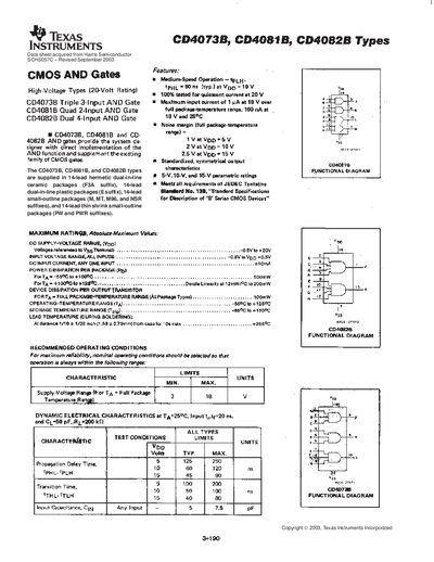
The CD4073B, CD4081B, and CD4082B are CMOS logic devices offering triple 3‑input AND, quad 2‑input AND, and dual 4‑input AND functions respectively. The sheet lists key features such as medium‑speed operation, typical propagation delays around 60 ns, and input capacitance of about 75 pF.
The document provides detailed package options (PDIP, SOIC, TSSOP, etc.), maximum ratings, recommended operating conditions, and ordering status (Active, NRND, etc.). Mechanical drawings and a package‑option addendum describe dimensions, lead layout, and environmental specifications.
| Input Capacitance (any input) | 75 pF |
|---|---|
| Maximum Supply Voltage | +70.5 V |
| Operating Temperature Range | -55 °C to +125 °C |
Each input has a capacitance of approximately 75 pF.