
The MAX7031 crystal-based, fractional-N transceiver is designed to transmit and receive FSK data at factory-preset carrier frequencies of 308MHz†, 315MHz, or 433.92MHz with data rates up to 33kbps (Manchester encoded) or 66kbps (NRZ encoded). This device generates a typical output power of +10dBm into a 50Ω load, and exhibits typical sensitivity of -110dBm. The MAX7031 features separate transmit and receive pins (PAOUT and LNAIN) and provides an internal RF switch that can be used to connect the transmit and receive pins to a common antenna. The MAX7031 transmit frequency is generated by a 16-bit, fractional-N, phase-locked loop (PLL), while the receiver's local oscillator (LO) is generated by an integer-N PLL. This hybrid architecture eliminates the need for separate transmit and receive crystal reference oscillators because the fractional-N PLL is preset to be 10.7MHz above the receive LO. Retaining the fixed-N PLL for the receiver avoids the higher current-drain requirements of a fractional-N PLL and keeps the receiver current drain as low as possible. The fractional-N architecture of the MAX7031 transmit PLL allows the transmit FSK signal to be preset for exact frequency deviations, and completely eliminates the problems associated with oscillator-pulling FSK signal generation. All frequency-generation components are integrated on-chip, and only a crystal, a 10.7MHz IF filter, and a few discrete components are required to implement a complete a
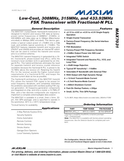
The MAX7031 is a compact 5 mm × 5 mm, 32‑pin thin QFN transceiver that provides factory‑preset carrier frequencies of 308 MHz, 315 MHz or 433.92 MHz for applications such as remote keyless entry, home automation, garage‑door openers and telemetry. It integrates separate transmit and receive PLLs, an internal RF switch, and requires only a crystal, a 10.7 MHz IF filter and a few discrete components.
Key electrical characteristics include typical output power of +10 dBm into a 50 Ω load, sensitivity of -110 dBm, supply voltage ranges of 2.1‑3.6 V (3 V mode) or 4.5‑5.5 V (5 V mode), and an automotive‑grade temperature range of -40 °C to +125 °C. Detailed pin descriptions, component values for typical application circuits, and package drawings are provided.
| Frequency Range | 308 MHz / 315 MHz / 433.92 MHz |
|---|---|
| Typical Output Power | +10 dBm into 50 Ω load |
| Typical Sensitivity | -110 dBm |
| Operating Temperature Range | -40 °C to +125 °C |
| Package | 32‑pin thin QFN, 5 mm × 5 mm |
The device supports factory‑preset carrier frequencies of 308 MHz, 315 MHz, or 433.92 MHz.
Typical output power is +10 dBm into a 50 Ω load.
The transceiver is specified to operate from -40 °C to +125 °C.