
This document describes the features and characteristics of a series of high-density NAND flash memory products, including memory capacity, supply voltage, page size, block size, read/write speed, etc.
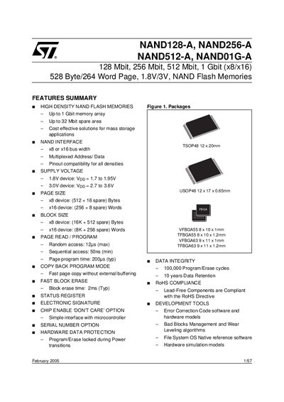
The NAND128‑A family comprises 128 Mbit, 256 Mbit, 512 Mbit and 1 Gbit SLC NAND flash devices available in x8 and x16 bus widths. Each device uses a 528‑Byte (512 + 16 spare) or 264‑Word (256 + 8 spare) page size and operates from a 1.8 V or 3.0 V supply. The architecture includes multiplexed address/data lines, reducing pin count and allowing density migration without footprint changes.
Key features include up to 100 000 program/erase cycles, 10‑year data retention, optional chip‑enable "don’t‑care" mode, a serial‑number option, and a copy‑back command for efficient defect management. Devices are offered in TSOP48, USOP48, VFBGA55, TFBGA55, VFBGA63 and TFBGA63 packages, all RoHS‑compliant.
| Memory Densities | 128 Mbit, 256 Mbit, 512 Mbit, 1 Gbit (x8/x16) |
|---|---|
| Page Size | 528 Bytes (512 + 16 spare) for x8, 264 Words (256 + 8 spare) for x16 |
| Supply Voltage | 1.8 V device: Vpp = 1.7‑1.95 V; 3.0 V device: Vpp = 2.7‑3.6 V |
| Block Size | x8: 16 KB + 512 B spare; x16: 8 KB + 256 Words spare |
| Random Access Time | 12 µs (max) |
| Sequential Access Time | 50 ns (min) |
| Page Program Time | 200 µs (typ) |
| Block Erase Time | 2 ms (typ) |
| Program/Erase Endurance | 100 000 cycles |
| Data Retention | 10 years |
| RoHS Compliance | Lead‑free components |
The devices can be powered at 1.8 V (Vpp = 1.7‑1.95 V) or 3.0 V (Vpp = 2.7‑3.6 V).
Each device is rated for up to 100 000 program/erase cycles.
The typical page program time is 200 µs.