
The IR2183(4)(S) are high voltage, high speed power MOSFET and IGBT drivers with dependent high and low side referenced output channels. Proprietary HVIC and latch immune CMOS technologies enable rugge- dized monolithic construction. The logic input is compatible with standard CMOS or LSTTL output, down to 3.3V logic. The output drivers feature a high pulse current buffer stage designed for minimum driver cross-conduction. The floating channel can be used to drive an N-channel power MOSFET or IGBT in bootstrap operation.
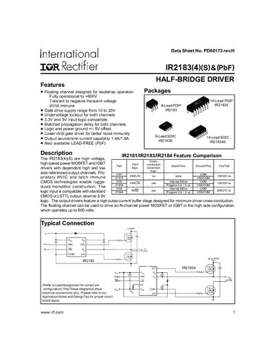
This datasheet describes the IR2183(4)(S) PbF half‑bridge driver, a high‑voltage, high‑speed MOSFET/IGBT driver with floating high‑side and low‑side channels. It lists key features such as a 10‑20 V gate‑drive supply range, 1.4 A/1.8 A source/sink capability, and lead‑free (PbF) options.
The document includes detailed electrical specifications, absolute maximum ratings, recommended operating conditions, functional block diagrams, pin assignments for various 8‑lead, 14‑lead PDIP and SOIC packages, and performance graphs covering propagation delay, rise/fall times, dead‑time, and logic input thresholds across temperature and supply voltage ranges.
| Gate drive supply range | 10 V to 20 V |
|---|---|
| Output source/sink current capability | 1.4 A source / 1.8 A sink |
| High‑side floating supply voltage (VB) | -0.3 V to 625 V |
| Output high short‑circuit pulsed current (IO+) | 1.4 A (typ) |
The driver operates with a gate‑drive supply voltage between 10 V and 20 V.
It can source up to 1.4 A and sink up to 1.8 A.
The high‑side floating supply can handle voltages from –0.3 V up to 625 V.