
This datasheet introduces the features of IR2105. IR2105 is a high voltage, high speed power MOSFET and IGBT driver with dependent high and low side referenced output channels. The device uses proprietary HVIC and latch immune CMOS technology, which has a rugged monolithic construction. The logic input is compatible with standard CMOS or LSTTL outputs. The output drivers feature a high pulse current buffer stage designed for minimum driver cross-conduction. The floating channel can be used to drive an N-channel power MOSFET or IGBT, in the high side configuration which operates from 10 to 600 volts.
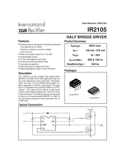
The IR2105 is a high‑voltage, high‑speed MOSFET/IGBT driver with floating high‑side and low‑side channels. It supports bootstrap operation, a gate‑drive supply of 10‑20 V, and includes built‑in dead‑time and undervoltage lockout.
The document lists absolute maximum ratings, recommended operating conditions, dynamic and static electrical characteristics, mechanical dimensions, and timing diagrams for both 8‑lead PDIP and 8‑lead SOIC packages.
| Maximum high‑side floating voltage (VB) | 625 V |
|---|---|
| Maximum VOFFSET | 600 V |
| Gate‑drive supply range | 10 V to 20 V |
| Typical turn‑on propagation delay | 680 ns |
| Typical turn‑off propagation delay | 150 ns |
| Typical dead‑time | 520 ns |
| Operating temperature range | -40 °C to 125 °C |
| Storage temperature range | -55 °C to 150 °C |
| Maximum junction temperature | 150 °C |
| Package options | 8‑Lead PDIP, 8‑Lead SOIC |
The device can tolerate up to 600 V on the high‑side floating channel.
Typical turn‑on propagation delay is 680 ns.
The IR2105 is offered in 8‑lead PDIP and 8‑lead SOIC packages.
The recommended ambient temperature range is –40 °C to 125 °C.